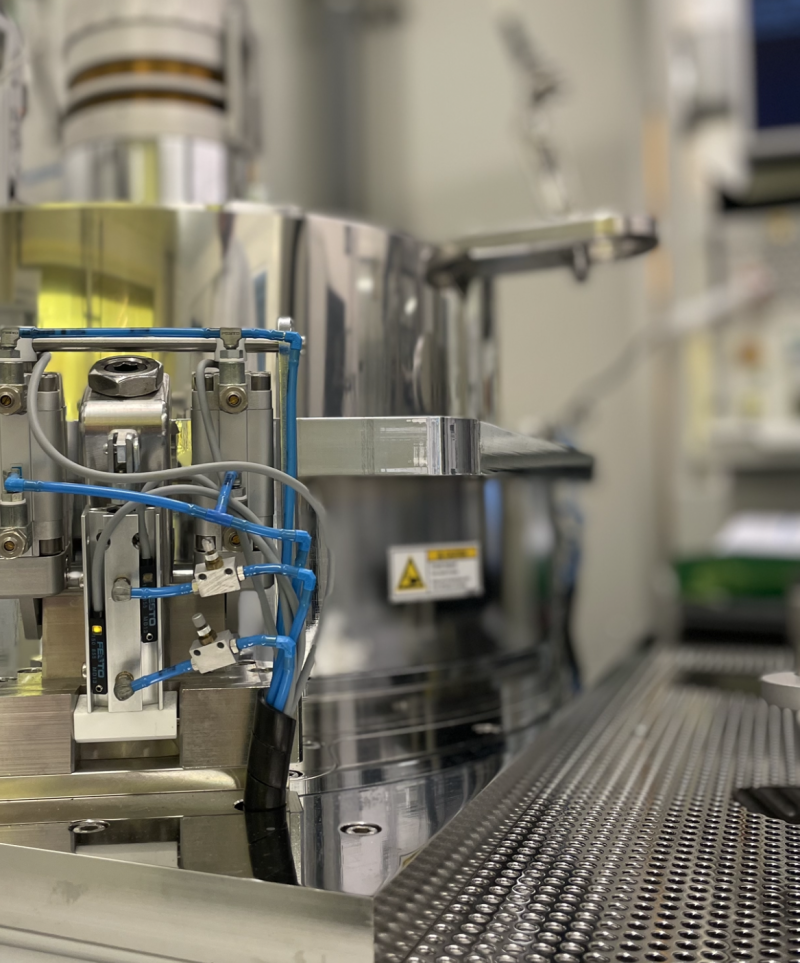
Our Wafer-Based Graphene Growth & Transfer Technology
Semiconductor devices (chips) are ubiquitous, with use ever-growing. The challenge for the industry is to continuously develop faster and better chips. For over 50 years, ‘Moore’s Law’, predicting that the number of components on a chip would double about every two years, has held. But current routes to innovation are reducing in effectiveness.
Traditionally, scaling – cramming more transistors on a chip – was the route to faster processing. But this approach is reaching the physical limits of current semiconductor technology. Novel 2D materials in combination with existing silicon address scaling challenges and push Moore’s law even further.
Many applications that aren’t driven by Moore’s law scaling, such as image sensors, photonics, MEMS, RF, power electronics, and sensing, can also benefit from the addition of novel materials. These are the so-called ‘More than Moore’ applications.
Graphene is a remarkable material – a sheet of carbon just one atom thick. The strongest substance in existence, it has outstanding electronic properties due to its two-dimensional nature. Incorporating graphene into chip technology can transform functional capability in areas such as power consumption and sensitivity. Over the next decade, combined with other 2D materials, graphene will take semiconductor technology to the next level.
However, there is a problem. Graphene has proved near-impossible to manufacture with the quality and consistency required by the semiconductor industry. ANL is the only company with the ability to produce and transfer to the chip high quality graphene at industrial scale.
For the past decade, we have developed the expertise and equipment to grow and stack high quality 2D material layers onto wafers. Our technology is now ready to produce high performance graphene layers in these ‘More than Moore’ applications.

Material growth
We have developed our own growth tools, substrates, and processes that allow us to grow the highest quality graphene to wafer sizes up to 200 mm. Our graphene is epitaxially grown in a unique process ensuring high quality and consistency. It is a pure, monolayer material with unprecedented strain and doping uniformity and a low wrinkle density.
Transfer
To get the graphene where it needs to be, we transfer it to a target substrate using an intermediate carrier in a process that is reminiscent of temporary wafer bonding and debonding technology. Some of the steps are unique, but the final integration to the customer substrate is made using commercially available bonding and debonding equipment. Because all the processing is wafer-based, we have ultimate control over the materials leading to fewer defects, better uniformity, cleaner interfaces, and a higher yield.
Device fabrication
The ANL foundry responds to the needs of fabless device manufacturers, integrated device manufacturers and other foundries. We offer a state-of-the-art foundry service for graphene device fabrication with a range of metallisation, lithography and encapsulation options. We also offer wafer scale device testing, and dicing if required.
Our technology is fully scalable, and we are expanding our fab capacity for graphene in 2023. This will increase our graphene layer production and wafer processing towards industrial volumes.
The 2D future
Graphene is the essential starting point for atom-thick materials in electronics, but other 2D materials are increasingly providing new opportunities. CMOS (Complementary Metal-Oxide Semiconductor) is currently the principal technology in chip manufacture – but ‘beyond CMOS’ applications that use new technologies for information processing and switching are opening up.
Our roadmap continues the development of 2D materials with the goal of producing the highest quality materials based on transition metal dichalcogenide monolayers (TMDCs). These typically consist of an atom-thick layer of transition metal (such as molybdenum or tungsten) sandwiched between two atom-thick layers of a chalcogen such as sulfur or selenium. Particularly when combined with graphene, TMDCs offer the potential to produce electronic devices that are smaller and more efficient than conventional electronics. What’s more they are also lower cost making them central to the next generation of devices.
Applied Nanolayers CVD in action
Experience the forefront of innovation in our video, where we showcase our cutting-edge CVD (Chemical Vapor Deposition) growth and transfer process, revolutionising graphene production. Our high-performance graphene is unlocking transformative applications in biosensors, photonics, and optoelectronic devices.
Connect with us
Interested in our technology or just looking for a conversation, feedback or discussion? Introduce yourself and let us know here.


